

Ion Beam Analysis (IBA)
Ion Beam Analysis (IBA) provides powerful, non-destructive characterization of thin films, interfaces, and advanced materials with exceptional quantitative accuracy. At JP Analytical, we combine multiple ion beam techniques to deliver depth-resolved compositional insight, enabling confident decisions in semiconductor R&D, process optimization, and failure analysis.
Using high-energy ion interactions with matter, IBA techniques measure elemental composition, thickness, areal density, and impurity distributions with minimal sample preparation — making them ideal for complex multilayer structures, ALD/PVD/CVD films, and emerging materials.
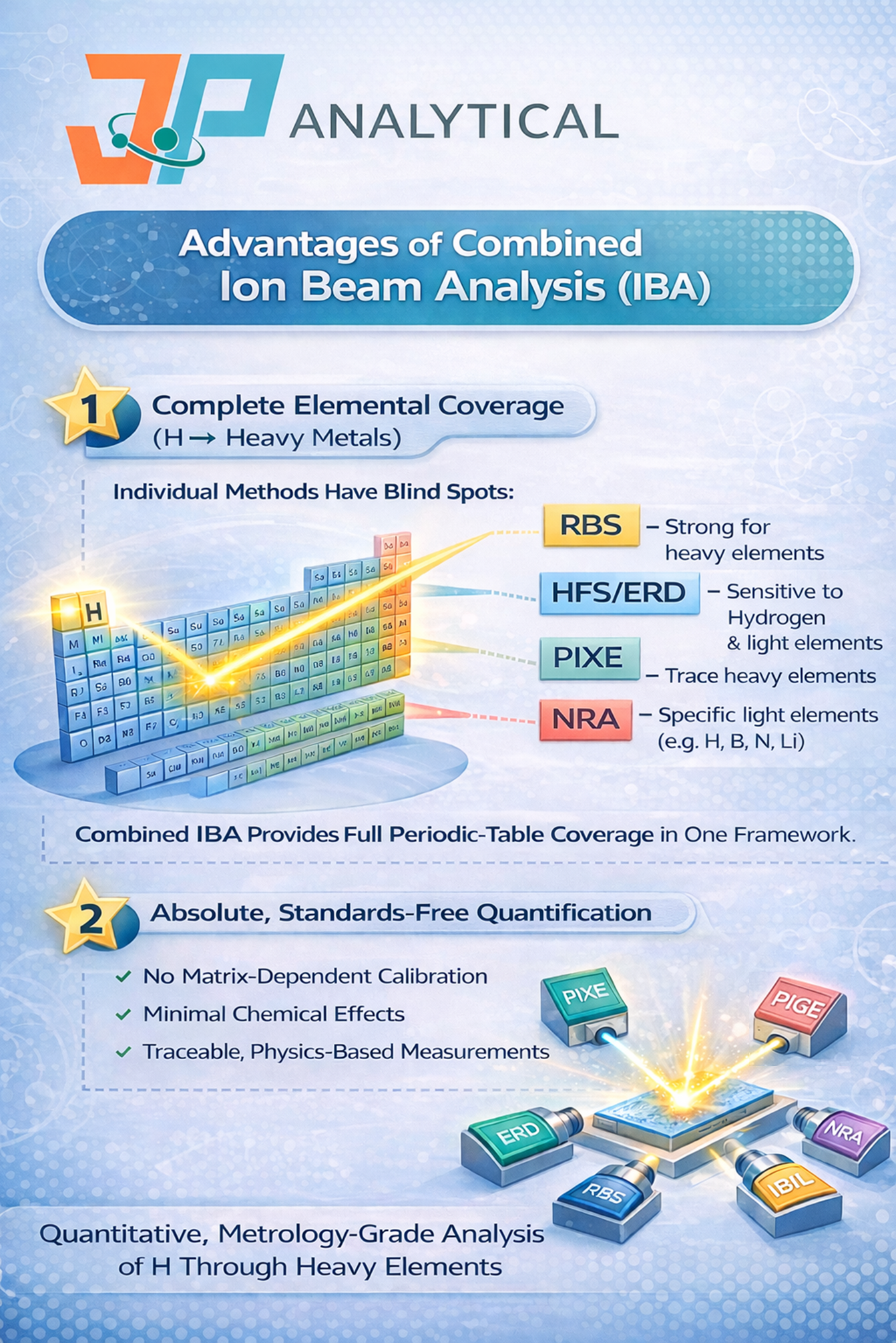
Our integrated approach emphasizes four core techniques:
Rutherford Backscattering Spectrometry (RBS)
RBS is the foundation of quantitative thin-film metrology. By analyzing the energy of ions backscattered from a sample, RBS provides:
Absolute stoichiometry and composition
Film thickness and density determination
Interface quality and diffusion profiling
Multilayer stack analysis with traceable quantification
RBS is especially valuable for semiconductor heterostructures, oxides, nitrides, and ALD-grown materials where precision and repeatability are critical.
Hydrogen Forward Scattering (HFS)
Hydrogen and light elements are often invisible to many surface techniques — but crucial to device performance. Our HFS capability enables:
Direct quantification of hydrogen and deuterium
Depth profiling of passivation layers
Evaluation of hydrogenation processes and defect passivation
Analysis of low-Z elements in advanced materials
HFS is particularly powerful for studying hydrogen-related defect engineering, thermal treatments, and reliability improvements.
Particle-Induced X-ray Emission (PIXE)
PIXE complements RBS by providing highly sensitive trace-element detection. Through ion-induced X-ray emission, PIXE delivers:
ppm-level elemental sensitivity
Rapid multi-element analysis
Contamination detection in semiconductor processes
Quantitative elemental mapping
This technique is ideal when trace impurities or metallic contaminants influence device yield and reliability.
Nuclear Reaction Analysis (NRA)
NRA enables selective detection of specific light elements using nuclear reactions with high depth resolution. Our NRA services support:
Precise hydrogen and deuterium profiling
Analysis of light elements such as nitrogen, oxygen, and lithium
Characterization of implantation and diffusion processes
Small-sample analysis where geometry limits other techniques
NRA is frequently used alongside RBS and HFS to provide a complete compositional and depth-resolved picture.
Why Combine Multiple IBA Techniques?
No single method captures the full complexity of modern thin films. By integrating RBS + HFS + PIXE + NRA, JP Analytical delivers:
Quantitative major-element analysis (RBS)
Hydrogen and light-element sensitivity (HFS & NRA)
Trace impurity detection (PIXE)
Cross-validated, publication-grade data
This combined methodology ensures reliable characterization for advanced semiconductor materials, energy devices, and emerging thin-film technologies.
Why Combine RBS + HFS?
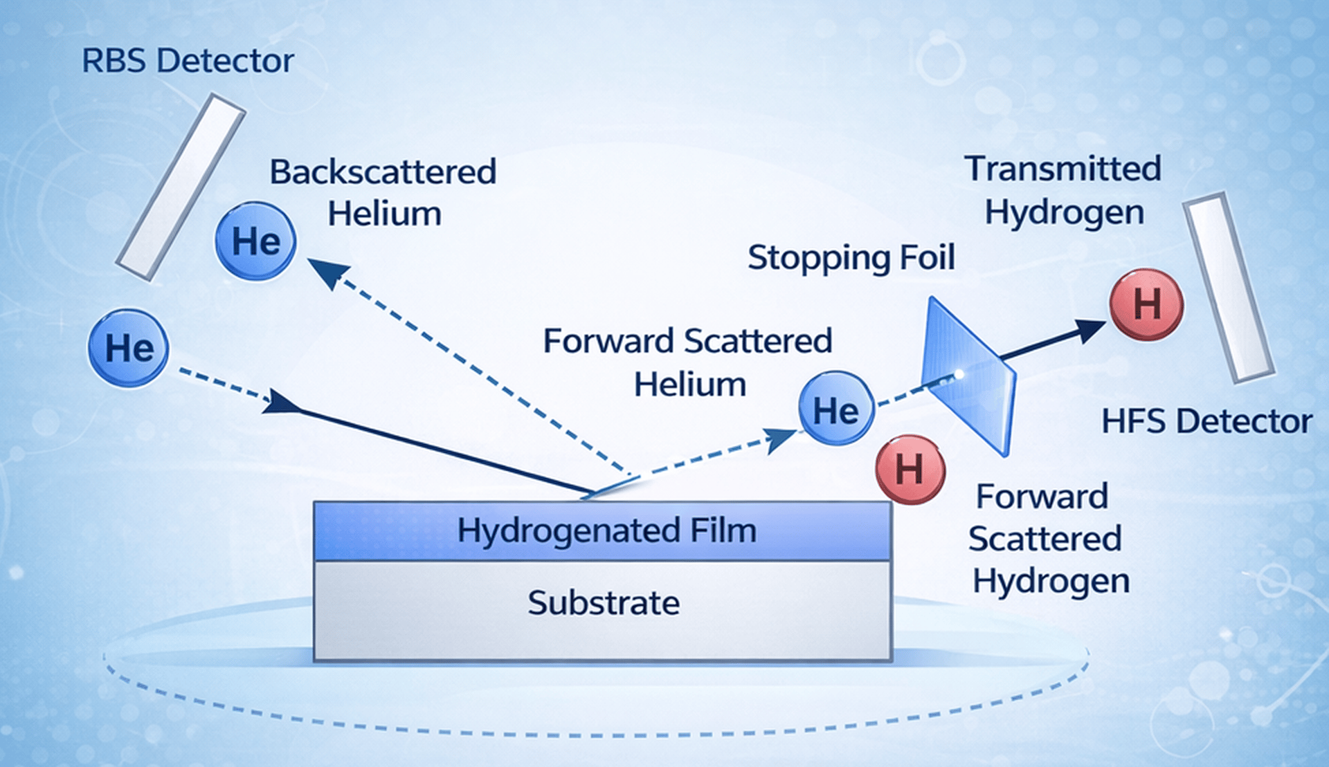
Modern thin-film materials often rely on both heavy-element precision and light-element control to achieve optimal device performance. While Rutherford Backscattering Spectrometry (RBS) delivers absolute quantification of composition, thickness, and density, Hydrogen Forward Scattering (HFS) uniquely reveals hydrogen and other low-Z elements that are invisible or difficult to measure with conventional methods. Combining these two complementary techniques provides a more complete and reliable understanding of complex material systems.
RBS + HFS together enable:
Complete elemental coverage – Quantitative analysis from heavy elements down to hydrogen
Accurate depth profiling – Correlating structural layers with hydrogen incorporation
Defect passivation insight – Direct evaluation of hydrogenation and thermal processing effects
Improved model accuracy – Reduced uncertainty through cross-validated measurements
Advanced device optimization – Understanding how hydrogen influences interfaces, strain, and electronic behavior
For semiconductor heterostructures, ALD/CVD multilayers, and emerging materials, the RBS+HFS approach provides a uniquely powerful dataset — linking structural composition with hydrogen-driven performance enhancements. This integrated methodology supports faster R&D iteration, higher process confidence, and deeper insight into failure mechanisms.
