Precision in Every Thin Film
JP Analytical delivers trusted metrology and R&D solutions tailored for semiconductor innovation.
Rated 4.9 stars
★★★★★
Who We Are
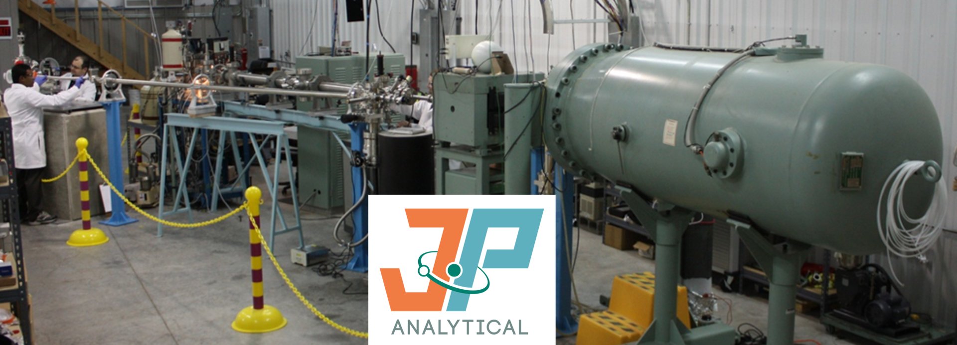
JP Analytical is a precision thin-film metrology and semiconductor R&D partner delivering quantitative, physics-based insight into advanced materials and devices. Through specialized characterization, defect passivation, thermal processing, and tailored research programs, we help innovators move from complex materials challenges to scalable technology with confidence.
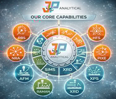
Our Services
Precision thin film metrology and semiconductor R&D tailored for your needs
Thin Film Analysis
Get precise measurements of film thickness and composition with our tailored Thin Film Metrology solutions. Enhance material performance through accelerator-based ion beam materials modification and analysis, ensuring optimal results for your applications.
Semiconductor R&D
Innovative Semiconductor R&D Solutions
Accelerating advanced materials and device development through precision metrology, defect engineering, and tailored research strategies.


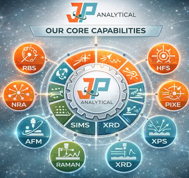
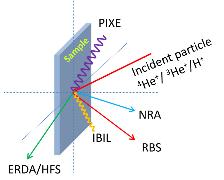
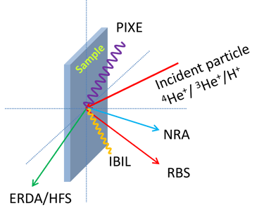
Ion Beam Analysis
Ion Beam Analysis (IBA) provides precise, non-destructive quantitative measurement of elemental composition, depth profiles, and thin-film properties with high sensitivity and minimal sample preparation.
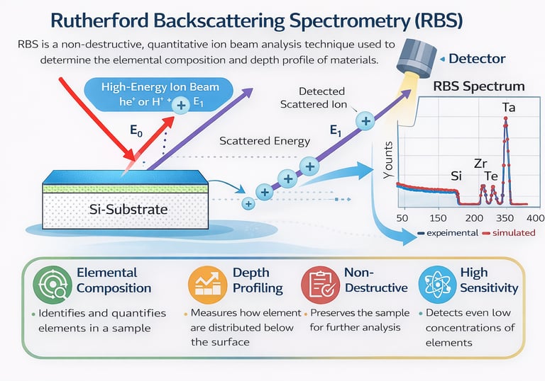
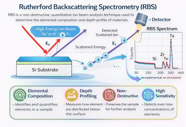
RBS
Rutherford Backscattering Spectrometry (RBS) is a non-destructive ion beam analysis technique that provides quantitative elemental composition, thickness, and depth profiling of thin films and materials.
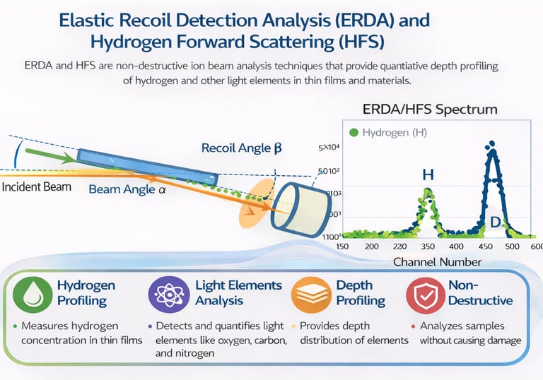
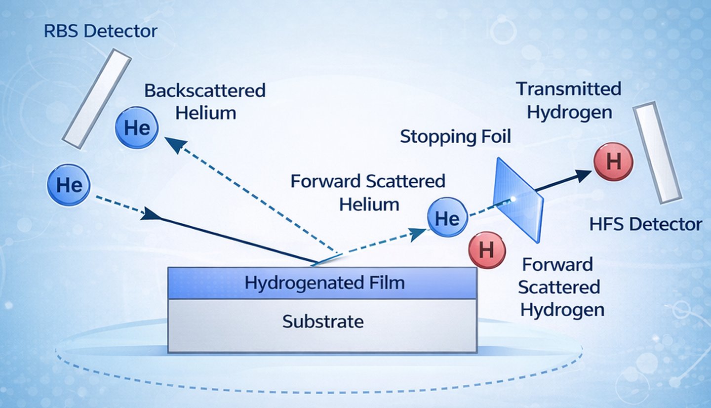
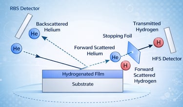
HFS and ERDA
ERDA/HFS is a quantitative ion beam analysis technique that enables sensitive, non-destructive depth profiling of hydrogen and other light elements in thin films and advanced materials.
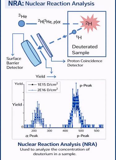
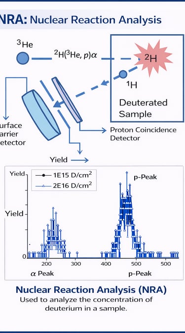
Nuclear Reaction Analysis (NRA) enables highly selective and quantitative detection of hydrogen and deuterium in thin films by measuring reaction products from the 2H(3He,p)α
NRA for Light Elements
RBS + HFS Why Combine?
At JP Analytical, we combine Rutherford Backscattering Spectrometry (RBS) with Hydrogen Forward Scattering (HFS / ERD) to deliver a truly comprehensive elemental and structural characterization of thin films and advanced materials. Individually powerful, these complementary ion beam techniques together provide full composition profiling—from hydrogen to heavy metals—with metrology-grade accuracy.
Complete Elemental Coverage — Including Hydrogen
RBS excels at quantifying medium-to-heavy elements and determining layer thickness, density, and interface quality. However, hydrogen and other very light elements are largely invisible to RBS. HFS fills this critical gap by directly measuring hydrogen (H), deuterium (D), and other light species with high sensitivity and depth resolution.
Together, RBS + HFS provide true stoichiometry across the entire periodic range (H → heavy elements) without assumptions or calibration standards.
Correlated Structure and Chemistry
By analyzing the same sample under controlled ion beam conditions, the combined dataset links:
Layer architecture and thickness (RBS)
Hydrogen content and distribution (HFS)
Interface quality and diffusion behavior
Absolute elemental concentrations
This integrated view is essential for understanding real material performance—not just composition in isolation.
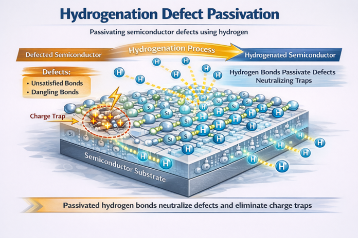
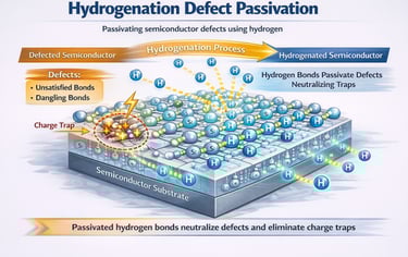
Detect Hidden Reliability and Process Issues
Hydrogen often governs device behavior yet remains undetectable by most conventional techniques. The RBS + HFS approach reveals:
Defect passivation effectiveness
Hydrogen incorporation during processing
Diffusion, trapping, and outgassing
Blistering and delamination precursors
Moisture uptake and contamination
These insights are critical for yield improvement, failure analysis, and process optimization.
Ideal for Advanced Semiconductor and Thin-Film Systems
Our combined RBS + HFS capability is particularly valuable for:
Semiconductor devices (Si, Ge, III-V, wide bandgap materials)
Gate dielectrics and passivation layers
Oxides, nitrides, and barrier coatings
Photovoltaic and energy materials
MEMS and microelectronics
Polymers and hydrogen-rich films
Metrology-Grade, Standards-Free Quantification
Because both techniques are based on well-understood ion–solid interactions, they provide absolute measurements without the need for reference standards. This makes RBS + HFS an ideal solution for research, process development, qualification, and independent verification.
Why Choose JP Analytical
JP Analytical delivers expert ion beam analysis with a focus on precision, reliability, and actionable insights for cutting-edge materials research and device development. Our integrated approach ensures you receive a complete, defensible characterization—not partial data.
RBS + HFS: See the structure. Measure the hydrogen. Understand the material.
Stay Informed
Get updates on thin film metrology and R&D